Time:2026-04-01 14:45:26Read:15
A pressure sensor is a device that converts pressure signals into measurable electrical signals and is widely used in industries such as industrial manufacturing, automotive, and medical care. The core component of a pressure sensor is the pressure-sensitive element, which detects changes in external pressure and converts them into changes in resistance or capacitance. Currently, there are two main types of pressure-sensitive elements: piezoresistive and capacitive. This article focuses on the fabrication process and applications of piezoresistive pressure-sensitive elements.
Fabrication Process of Piezoresistive Pressure-Sensitive Elements
The fabrication process of piezoresistive pressure-sensitive elements mainly includes the following steps:
Wafer Preparation: The wafer serves as the base material for semiconductor devices. Silicon is typically used as the raw material, and the wafer is produced through processes such as polysilicon growth, slicing, and polishing. The diameter and purity of the wafer determine the performance and yield of the devices^1^.
Ion Implantation: Ion implantation is the process of forming semiconductor resistors on the wafer surface. A high-energy ion beam is used to implant dopants into the silicon layer, thereby modifying its conductivity^2^. The process involves two implantation steps: heavy doping and light doping. Heavy doping forms the four heavily doped regions of the Wheatstone bridge, while light doping forms the four piezoresistive strips^3^.
Silicon Trench Etching: Silicon trench etching is the process of forming trenches on the backside of the wafer. Wet anisotropic etching is used to partially remove the silicon layer, creating a thin film in the sensitive area on the wafer surface^2^. The depth and shape of the silicon trench affect the sensitivity and linearity of the sensitive element^3^.
Wafer-Level Packaging: Wafer-level packaging involves bonding glass layers to both the top and bottom surfaces of the wafer. An anodic bonding technique is used to tightly bond the glass layers to the silicon layer, forming a "glass-silicon-glass" three-layer structure^2^. The glass layers provide protection and isolation, as well as serving as feedthrough holes and housing a temperature-sensing diode^3^.
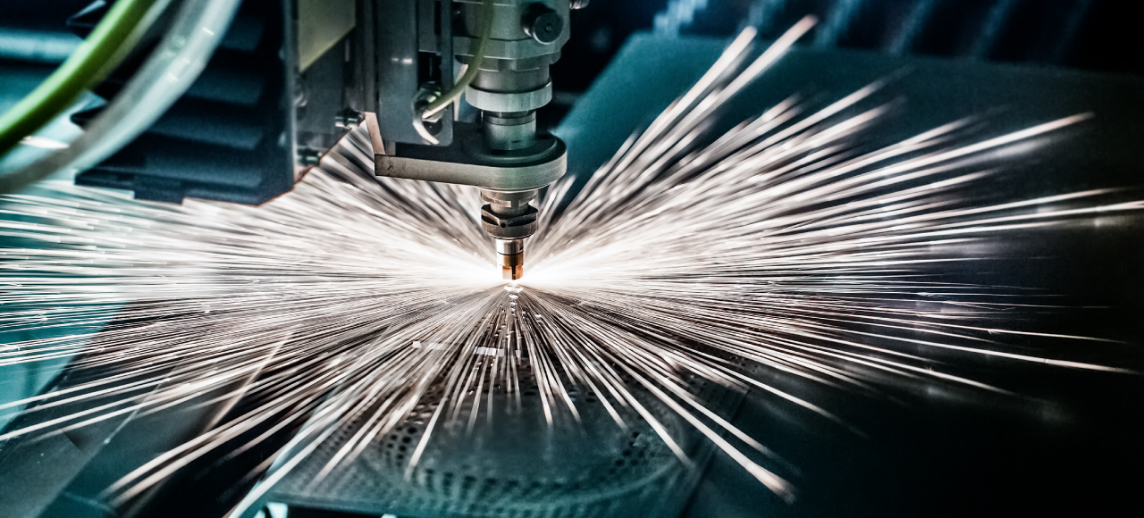
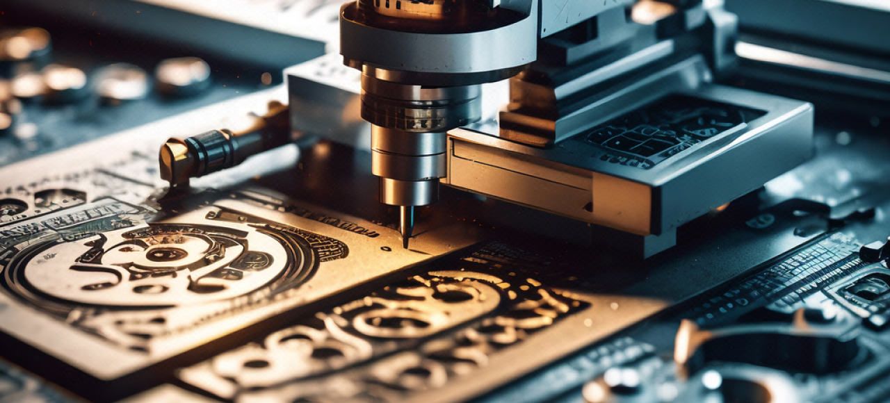
Die Singulation: Die singulation is the process of cutting the wafer into individual chips. This is done using a diamond blade or laser cutting technology along predefined scribe lines^1^. After singulation, the chips undergo subsequent processing steps such as cleaning, inspection, and sorting.
Applications of Piezoresistive Pressure-Sensitive Elements
Piezoresistive pressure-sensitive elements offer advantages such as a simple structure, fast response, stable output, and high-temperature tolerance, making them suitable for pressure measurement in air, liquids, and harsh gas environments^3^. They can be packaged with circuit chips, PCBs, metal casings, and other components to form various types of pressure sensors to meet the needs of different fields. For example:
Industrial Field: Pressure sensors are used in HVAC systems, industrial automation, process monitoring, water level and pressure monitoring, etc., improving production efficiency and safety^3^.
Automotive Field: Pressure sensors are used for transmission oil pressure, fuel system pressure, tire pressure, brake system pressure, etc., enhancing vehicle performance, energy efficiency, and environmental protection^3^.
Medical Field: Pressure sensors are used in diagnostic and analysis equipment, hemodialysis machines, ventilators, blood pressure monitors, etc., improving medical quality and patient comfort^3^.
PREVIOUS:Danaher Setra has newly launched the Model 278 atmospheric pressure sensorNEXT:How Scientists Use Thermal Cameras to Predict Volcanic Activity Changes